Comments? email to
![]()

![]()
 A
legal-limit (1500w) version of this amplifier, using the MRF1K50,
is documented at this bookmark, as is an
RF deck using the MRFX1K80H (1800w @ 65V device)
A
legal-limit (1500w) version of this amplifier, using the MRF1K50,
is documented at this bookmark, as is an
RF deck using the MRFX1K80H (1800w @ 65V device)
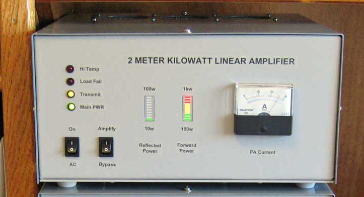
The original 1kw amplifier article was published in QST magazine (October 2012)
 It's
hard to beat a kilowatt for annoying your neighbors and some of your fellow
contesters during those big events; I'm joking, of course, this one is very
stable, clean, quiet in operation, yet compact and full-featured. It has a lot of
gain, requiring only about 2w drive for 1kw out, is over 70% efficient at that
level, and will go a bit more if need be; I was able to get a little over 1200w
saturated output at higher drive levels, but 1kw is the practical limit for
linear operation.
It's
hard to beat a kilowatt for annoying your neighbors and some of your fellow
contesters during those big events; I'm joking, of course, this one is very
stable, clean, quiet in operation, yet compact and full-featured. It has a lot of
gain, requiring only about 2w drive for 1kw out, is over 70% efficient at that
level, and will go a bit more if need be; I was able to get a little over 1200w
saturated output at higher drive levels, but 1kw is the practical limit for
linear operation.
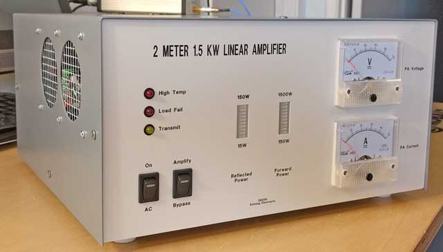
There are some handy features in this one:
- Compact cabinet design (6 x 12 x 12 inches)
- Full VSWR and over-temperature protection
- Metering for PA current, with peak-reading LED bar graph meters for forward and reflected power
- Full t/r sequencing
- Low-loss high-power antenna relays
- ALC output for the driver
- Rear panel jumpers for selecting low power drive levels, or for up to 50w drive using a built-in 50w 10db attenuator
- Low-noise temperature-controlled cooling fans
- Front-panel AC switch for it's external power supply
It uses a single 50v LDMOS transistor made by Freescale Semiconductor, the MRFE6VP61K25H. The device is normally used in a push-pull configuration (it's a dual-device part), and the data sheet lists it as a 1.8 to 600 MHz unmatched device. In fact, this document shows component values and board layout for a 230 MHz amplifier, and that prompted me to try the device on the 222 MHz band as well; results were similar, though gain was a bit lower at saturation (24db); still, only 4w drive for a kw out on 222MHz isn't bad.
Changes since this article was written:
 Since this
article was originally written, I made a few
enhancements; the amplifier now has a
newer control board that combines additional features formerly provided by
other assemblies, and the entire amp can be run with just 50v (the 12 and 28v
are derived inside the cabinet from 50v). Now there is also a sequenced LNA
power feed, and I've also constructed
KW RF decks using the
NXP BLF578XR LDMOS device, with the same results. Very minor changes in
matching components and bias levels need to be made (info
on one of these RF decks is here). Another more recent part, the NXP
BLF188XR, can be substituted without any changes whatsoever.
Since this
article was originally written, I made a few
enhancements; the amplifier now has a
newer control board that combines additional features formerly provided by
other assemblies, and the entire amp can be run with just 50v (the 12 and 28v
are derived inside the cabinet from 50v). Now there is also a sequenced LNA
power feed, and I've also constructed
KW RF decks using the
NXP BLF578XR LDMOS device, with the same results. Very minor changes in
matching components and bias levels need to be made (info
on one of these RF decks is here). Another more recent part, the NXP
BLF188XR, can be substituted without any changes whatsoever.
The low pass filter, Narda coupler and dual detector pcb have also been replaced with a single assembly combining all of these parts; this combination assembly can be set up for 6m, 2m, 222 MHz or 70cm. This next photo shows the inside, the way I currently build them.
A complete Bill of Materials (BOM) for the
1kw turn-key amplifier, configured as I currently build them, is listed at the
end of this article.
 The original work on the 2m amplifier core was developed and
written up in Dubus magazine by F1JRD, and much information can be retrieved
with an internet search on his call sign. Additional information on this is on F1JRD's web site. I built the amplifier
sub-assembly as documented there (with a couple of minor changes), and it worked
as published. However, I did make some improvements to the board in bias control
and matching component durability (important for WSJT users), and I have
kits available for the newest RF deck and other assemblies
available on the parts page.
The original work on the 2m amplifier core was developed and
written up in Dubus magazine by F1JRD, and much information can be retrieved
with an internet search on his call sign. Additional information on this is on F1JRD's web site. I built the amplifier
sub-assembly as documented there (with a couple of minor changes), and it worked
as published. However, I did make some improvements to the board in bias control
and matching component durability (important for WSJT users), and I have
kits available for the newest RF deck and other assemblies
available on the parts page.
The photo on the right is the first prototype, and the one
featured in the magazine article.
Inside
the cabinet, you can't help but notice how small the amplifier core really is
(it measures 3 inches by 5 inches). The copper heat spreader it's mounted to is
pretty thick (mine is .625 thick), and then the spreader is mounted to a large
piece of Aluminum heat sink.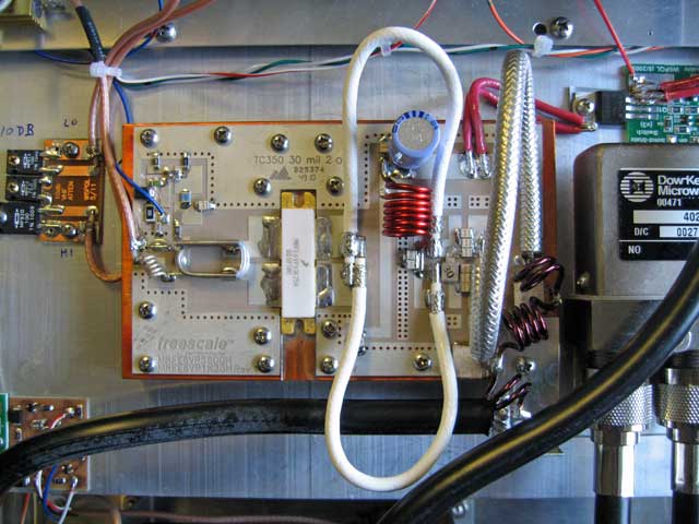
The transistor has provisions for mounting with screws, but I chose to flow-solder it to the copper spreader for best thermal transfer. The original plans also recommended flow-soldering the board to the spreader, but because this is 2m, I didn't bother doing that; I just held it in place with screws, and there were no problems.
The 3 small coils at the output (next to the output antenna relay) are part of a low-pass filter, and not part of the kit. I built this on a small piece of tin sheet and held it in place with a couple of the board mounting screws. Details for making this filter are on the schematic shown later in this article.

As can be seen on the analyzer display to the right, the filter does a good job of keeping the output harmonics well within FCC regulations.
For this measurement, output was sampled at 1kw out, using a directional coupler and attenuators to keep from overloading the input of the spectrum analyzer.
 One of the minor modifications I made
(shown at left) was to use a Dremel tool
to make a few more pads out of a couple of larger ones at the upper left of the
board; I did this to attach additional components for an adjustable bias circuit
(the small trimmer pot in the center) for setting the proper IDQ.
One of the minor modifications I made
(shown at left) was to use a Dremel tool
to make a few more pads out of a couple of larger ones at the upper left of the
board; I did this to attach additional components for an adjustable bias circuit
(the small trimmer pot in the center) for setting the proper IDQ.
Another small change was eliminating the ferrite
bead in the bias return; there were no reported stability problems by other
builders, but I've had trouble with using them in
input circuits before, so I decoupled with resistors and caps instead, just to
be safe. Other builders of the kit reported failure of the two 15pf ATC
capacitors in the output matching circuit (they caught on fire and burned like a
torch), so I used a 30pf metal mica there (type J601). Rf currents are high in
some areas, particularly the output matching network, and the metal micas are
better able to handle these conditions; the ATC types are OK for D.C. blocks.
After these photos were taken, I also replaced the 22k resistor in the bias
circuit with a 5k, and added a 5k thermistor in parallel with that. These parts
were added to control a rise in idle current as the transistor heated up on long
transmissions. The only other change I can think of right now was the
electrolytic bypass capacitor on the VDD supply line ( I used a single 220uf
part there).
 The kit of parts came with two pieces of 10 ohm coax, and one
piece of 50 ohm .250 semi-rigid for the output baluns/matching transformers. I
make mention of this because, as supplied in the kit, these coax pieces were a
couple cm longer than the article specified. I pondered this, and decided not to
trim them shorter, reasoning that at 2m, it wouldn't matter much. It didn't, but
after asking another builder about this (F5BQP), who was kind enough to send me
info on trimming them (shown at right), I went back later and trimmed them to
spec just to be certain I wasn't missing anything after all. The amplifier
played pretty much the same, but the input match was degraded (typical of
amplifiers when you retune the output). To fix this, I eliminated L1 (the input
matching inductor) and just fed the input balun directly. Input return loss
improved to about 17db, or 1.35 to 1, quite acceptable.
The kit of parts came with two pieces of 10 ohm coax, and one
piece of 50 ohm .250 semi-rigid for the output baluns/matching transformers. I
make mention of this because, as supplied in the kit, these coax pieces were a
couple cm longer than the article specified. I pondered this, and decided not to
trim them shorter, reasoning that at 2m, it wouldn't matter much. It didn't, but
after asking another builder about this (F5BQP), who was kind enough to send me
info on trimming them (shown at right), I went back later and trimmed them to
spec just to be certain I wasn't missing anything after all. The amplifier
played pretty much the same, but the input match was degraded (typical of
amplifiers when you retune the output). To fix this, I eliminated L1 (the input
matching inductor) and just fed the input balun directly. Input return loss
improved to about 17db, or 1.35 to 1, quite acceptable.

Looking down from the top of the amp, at bottom center is a surplus Narda dual directional coupler, a 30db coupler normally used at 900 MHz, it is quite broadband, and has a coupling factor of about 42db at 144 MHz, just right for monitoring forward and reflected power at the kw level. The sampled signals are routed to a detector board shown later.
Note the use of ferrite beads and bypass capacitors on the power connector, and the ALC and PTT connectors. The ammeter and LED meters are also fed in this manner.
At the left of the copper spreader is the 50w 10db attenuator, used for higher power drivers. This attenuator is made using non-inductive (at 2m) TO-220 style resistors, and is jumpered in via rear panel bulkhead connectors. The attenuator is out of the bypass path, and is only in-circuit following the input antenna switch, and routed through the input jumpers to the amplifier board.

A setup table listing various attenuator values can be found here:
LMR-400 is used for all of the high power jumper connections (good to 1.5 KW continuous at 150 MHz). Though UHF connectors are common at this frequency, I used type N and SMA everywhere. Not important, I just happen to like them better, BNC and UHF connectors would have been fine.
 Looking
at the rear panel shows the connectors provided for moving the 10db attenuator
in or out of the input path. There is also a screwdriver adjustment for setting
the ALC level.
Looking
at the rear panel shows the connectors provided for moving the 10db attenuator
in or out of the input path. There is also a screwdriver adjustment for setting
the ALC level.
Also visible here are the 4 small cooling fans behind the
screened vent holes. Cool air is drawn in here, forced through the heat sink
fins inside, and then expelled out the top of the cabinet through additional
screened vents (just visible here in the cabinet cover). These fans run at
reduced speed (to keep them quiet) during the transmit cycle, and will also run
continuously if the heat sink temperature rises above 115F. Should the
temperature rise above 130F, the fans will run at full speed, and the amplifier
will lock itself into bypass mode until it cools down to about 120F; then it
will unlock itself again and operate normally. I haven't been able to get it
that hot yet, but the protection is there just in case.
 A
snapshot of the right side shows the two antenna switches and the method for
mounting the cooling fans.
A
snapshot of the right side shows the two antenna switches and the method for
mounting the cooling fans.
Brackets for holding the directional coupler are made from .060 Aluminum, and held to the cabinet floor with screws.
A high-current FET switch, shown just to the right of the large antenna switch, gates the 50v VDD to the amplifier. This allows the control board sequencer to turn it on and off at the correct times.
There is a small bracket holding the LED bar graph meters in place on the front panel, mounted in a way that avoids having to drill mounting holes into the panel. It's held in place to the top and bottom lips of the panel with counter-sunk 2-56 screws. A better view of this is shown in the inset below:

 On
the other side, the control board is visible at bottom center, as is the
RF
detector board to it's left, which is used to detect the signals from the
directional coupler and drive the power meters and SWR lockout switch on the
control board.
On
the other side, the control board is visible at bottom center, as is the
RF
detector board to it's left, which is used to detect the signals from the
directional coupler and drive the power meters and SWR lockout switch on the
control board.
Even though the LDMOS transistor will handle 65 to 1 VSWR without failing (it's very tough), many of the other components, including the antenna switches and coax, can't survive the extreme voltages this would place on the transmission lines; so I set the SWR lockout adjustment at 100w reflected power, or about 2 to 1 VSWR at 1kw out. When tripped, this feature will lock the amplifier in bypass mode until manually reset (main power must be turned off for several seconds to reset it).
I'm sure glad I put that SWR lockout on there; while doing some offline testing, I forgot to hook up the output coax. I really didn't intend to test it at 1kw without a load, but it happened, and it locked out the amp just like it was supposed to do. No damage, even after I managed to do it again about an hour later.
The small PC board on the heat sink above and to the right of the control board is the high-temp lockout switch.
 This
last photo shows the amplifier operating at full output. My antenna isn't
perfect, and the 10w reflected power is evident on one of the LED bar graph
displays.
This
last photo shows the amplifier operating at full output. My antenna isn't
perfect, and the 10w reflected power is evident on one of the LED bar graph
displays.
A set of schematics, as well as front/rear panel sketches can be seen by clicking here.
The block diagram for the most current version of the turn-key amp can be seen here.
If you are building the RF deck from a kit I supplied, the assembly instructions are here.
For kits shipped after Sept. 10th, 2018, your instructions are here.
For kits shipped after September
2020, your instructions are here.
 Rack-mounting
the amp is another way to go if you like your equipment set up that way.
Rack-mounting
the amp is another way to go if you like your equipment set up that way.
This one was built with an engraved front panel and dual
meters of a slightly different style..
What follows here is a complete Bill of Materials for the standard 1 KW amplifier:
The cabinet consists of the front and rear panels and a floor plate I have
made by Front Panel Express (FPE,
www.frontpanelexpress.com);
they have design software you can download for free, which allows you to design
custom panels and order them through their system. Their CNC machining process
does all the hole cutting and engraving of those parts, and the panels can be
ordered in a powder-coat or anodized finish.
The wrap-around cover and internal support brackets and tie-ins I make here; the
standard color I use is light gray with a medium gray cover, but if you want to
match existing equipment, many other color schemes are available (black anodized
finish with white lettering for example). You can expect to pay about $275 for
the panels if ordered directly from Front Panel Express, and the rest of the
parts to make the cabinet will cost around $175 if I make them here, plus
shipping for the completed cabinet. If you have your own sheet metal tools
(shear and bending brake), you can save some $ there. Domestic shipping for the
finished cabinet has been running 30 to $50 (depends on where you are) using FedEx ground service.
If you want to go the Front Panel Express way, a block diagram of the amplifier, and my design files for the panels mentioned above can be found in this folder.
| description | p/n | quantity | supplier |
| #10 THHN stranded wire, black | 15ft | Ace hardware | |
| #10 THHN stranded wire, red | 15ft | Ace hardware | |
| #14 THHN stranded wire, blue | 5ft | Ace hardware | |
| #14 THHN stranded wire, red | 5ft | Ace hardware | |
| #18 THHN stranded wire, red | 5ft | Ace hardware | |
| White rubber feet, 4 per pack | 1 pack | Ace hardware | |
| multi-conductor hook-up wire, 10ft | 10cs22 | 10ft | Allelectronics |
| meter, panel, 100V DC | PMD-100V | 1 | Allelectronics |
| meter, panel, 50A DC | PMD-50A | 1 | Allelectronics |
| meter shunt, 50A | snt-50 | 1 | Allelectronics |
| 5mm led, red | LED-1 | 2 | Allelectronics |
| 5mm led, yellow | LED-3 | 1 | Allelectronics |
| 5mm led, green | LED-3 | 1 | Allelectronics |
| 60mm fan, 17cfm, 12v |
|
5 | Allelectronics |
| sma jack for rg174/rg316 | Ebay | 4 | Ebay |
| sma plug for rg174/rg316 | Ebay | 4 | Ebay |
| rg142 coax, 5ft | Ebay | 1 | Ebay |
| rg316 coax, 6ft | Ebay | 1 | Ebay |
| flat washer, #4 | 90126a505 | box of 100 | McMaster-Carr |
| flat washer, #6 | 90126a509 | box of 100 | McMaster-Carr |
| flat washer, #8 | 90126a512 | box of 100 | McMaster-Carr |
| flat washer, 1/4" (thin) | 90945a760 | 1 | McMaster-Carr |
| k/l nut, 4-40 | 90675a005 | box of 100 | McMaster-Carr |
| k/l nut, 6-32 | 90413a101 | box of 100 | McMaster-Carr |
| k/l nut, 8-32 | 90675a009 | box of 100 | McMaster-Carr |
| lock washer, internal, 1/4" | 91113a029 | 1 | McMaster-Carr |
| machine screw, 4-40 x 1/2 | 90272a110 | box of 100 | McMaster-Carr |
| machine screw, 4-40 x 1/4 | 90272a106 | box of 100 | McMaster-Carr |
| machine screw, 4-40 x 3/16 | 90272a105 | box of 100 | McMaster-Carr |
| machine screw, 4-40 x 3/4 | 90272a113 | box of 100 | McMaster-Carr |
| machine screw, 4-40 x 3/8 | 90272a108 | box of 100 | McMaster-Carr |
| machine screw, 6-32 x 3/8 | 90272a146 | box of 100 | McMaster-Carr |
| machine screw, 6-32 x 3/4 | pack of 10 | Local hardware store | |
| machine screw, 8-32 x 3/4 | 90272a197 | box of 100 | McMaster-Carr |
| phillips screw, sheet metal, #6 x 3/8 | 91775a640 | box of 100 | McMaster-Carr |
| Panel clip for 5mm LED | CR-174 | 4 | Mouser |
| #6 solder lug | 7326 | 10 | Mouser |
| 12 ohm 50w metal-cased resistor | rh50-12 | 1 | Mouser |
| 24v spdt relay | T9AP5D52-24 | 1 | Mouser |
| 25 ohm 25w metal-cased resistor | rh25-25 | 1 | Mouser |
| 250 ohm 25w metal-cased resistor | rh25-250 | 1 | Mouser |
| 3.5mm mono jack | 161-3142m-e | 1 | Mouser |
| 3.5mm mono plug | 171-PA3191-1-E | 1 | Mouser |
| 30a bridge rectifier | mp251 | 1 | Mouser |
| 4700 pf 50v 1206 capacitor | VJ1206Y472MXAPW1BC | 4 | Mouser |
| 5.1k 1206 resistor | CRCW12065K10JNEA | 1 | Mouser |
| 560 ohm 3w resistor | RSS3560RJTB | 1 | Mouser |
| anderson power pole cable clip pkg | 115g7 | 1 | Mouser |
| anderson power pole cable housing, 2x2 | 1460g1 | 1 | Mouser |
| anderson power pole chassis shell, 2x2 | 1470g1 | 1 | Mouser |
| anderson power pole contact, 30A | 1331 | 4 | Mouser |
| anderson power pole contact, 45A | 261g2 | 4 | Mouser |
| anderson power pole housing, black | 1327g6 | 2 | Mouser |
| anderson power pole housing, blue | 1327g8 | 4 | Mouser |
| anderson power pole housing, red | 1327 | 2 | Mouser |
| anderson power pole retaining pin | 110g9 | 1 | Mouser |
| ferrite core | 28b0375-000 | 50 | Mouser |
| ferrite core | 28b0562-100 | 30 | Mouser |
| molex .062 contact, female | 02-06-1103 | 27 | Mouser |
| molex .062 contact, male | 02-06-2103 | 27 | Mouser |
| molex .093 contact, female | 02-09-1104 | 6 | Mouser |
| molex .093 contact, male | 02-09-2103 | 6 | Mouser |
| molex plug, 6 circuit, .093 | 03-09-2061 | 1 | Mouser |
| molex plug, 9 circuit, .062 | 03-06-2091 | 1 | Mouser |
| molex receptacle, 6 circuit, .093 | 03-09-1061 | 1 | Mouser |
| molex receptacle, 9 circuit, .062 | 03-06-1092 | 1 | Mouser |
| phono jack | 16pj052 | 1 | Mouser |
| rocker switch, 15A | r1966ablkblkfs | 2 | Mouser |
| spacer, 1/4" for #4 screw | 398 | 12 | Mouser |
| spacer, 3/8" for #6 screw | 407 | 8 | Mouser |
| terminal, .187 tab, 18-22 awg | 159-2187 | 2 | Mouser |
| terminal, .250 tab, 16-14 AWG | 8-696302-1 | 7 | Mouser |
| terminal, for #8-10 screw, 12-10 AWG | 35109 | 3 | Mouser |
| N connector, bulkhead for RG316 | 172129 | 1 | Mouser |
| N connector, bulkhead for RG142 | 172132 | 1 | Mouser |
| heat sink, 10 x 6 x 3.5, 6 pounds weight | HS-machined | 1 | Heat Sink USA |
| Bar graph display support bracket | supplied with cabinet fitting | 2 | W6PQL |
| copper spreader, 3 x 5 x 1/2 | CS-machined | 1 | W6PQL |
| flat washer, #5 | supplied with FET switch kit | 2 | W6PQL |
| input attenuator, 6, 10, 13 or 16db | INATTEN | 1 | W6PQL |
| Kit, bar graph display, red, green, or tri-color | BARGRAPH | 2 | W6PQL |
| kit, basic 2m kw amplifier | 2MKWAMPKIT | 1 | W6PQL |
| kit, control board | CTRL-v6.2 | 1 | W6PQL |
| kit, high current fet switch | HCFS | 2 | W6PQL |
| kit, low pass filter w/dual detectors | LPF | 1 | W6PQL |
| kit, ALC board | ALC | 1 | W6PQL |
| LED pcb, 4 position | LEDPCB | 1 | W6PQL |
| LPF support bracket and shield | supplied with cabinet fitting | 1 | W6PQL |
| relay, rf input | relayin | 1 | W6PQL |
| relay, rf output w/2m comp capacitors | relayout2m | 1 | W6PQL |
| ldmos, blf188xr | blf188xr | 1 | W6PQL |
A 1500w (legal-limit) 2m LDMOS Amplifier
This first photo shows two different versions of this amplifier in a couple of the more popular color schemes. The gray one on the left uses a 50v 1500w device, and will produce sustained 1.5kw in SSB/CW modes but must be limited to about 1200w for JT65 EME and other digital modes. This limitation is due to the matching transformers having an upper limit on how much power they can handle without getting so hot as to melt the solder holding them in place. Since SSB and CW duty cycles are no more than about 50% max, 1.5kw is no problem...but sustained digital modes will cause them to overheat.
The second amplifier on the right uses two 1kw RF decks with a combiner, a larger heat sink and a more ruggedized LPF. This one is capable of 1500w in all modes, including the more demanding digital modes (JT65 and others) used for EME. Absolute maximum output on this one, measured at 51v and max drive was 2.5KW. Of course, this was into a dummy load, and not for very long (about as long as my nerves could stand it).


For this 2-deck amp, 44v produced the best efficiency while preserving excellent linearity at legal limit; as you can see in the graph, at 1500w we are not even at P1db...there is still "headroom".
Even at 1650w we remain just below P1db, and linearity is still very good.
Naturally, with each RF deck producing less than 1kw, the rf transformers are not stressed at all. The combiner handles the high power work, and is rated well beyond 2kw.
The input power listed in these graphs was applied through a 13db transmit-side
attenuator, as the driving radio was a 100w model. This reduced the maximum 100w
drive level to 5w at the input of the two rf decks (2.5w each)

At 50v, linearity is preserved all the way to 2kw, but at the cost of a few % points of efficiency.
These amplifiers are most efficient when they are close to saturation, and that
is the reason for backing down VDD on this 2-deck model to the reduced level of
44v as shown in the previous graph.

Here's a snapshot of the interior, showing the placement of many of the major
assemblies.

And a more detailed view of the front panel. The rear panel layout is similar to the single-deck model below, but this one has four high-volume fans for cooling, a total of 240 cfm.
The cabinet size is 15w by 15d by 7h.
Now back to the single-deck model:
 Some
time after the MRF1k50 became available, I thought it might be nice to see if it
really would do 1500w...it did. A nice bonus was the discovery it was able to do
that with reasonable IMD3 performance (-30dbc at 1500w). It required a bit more
drive, but not much more (4 to 5w) to get there, and drew about 42 amps at 50v.
Some
time after the MRF1k50 became available, I thought it might be nice to see if it
really would do 1500w...it did. A nice bonus was the discovery it was able to do
that with reasonable IMD3 performance (-30dbc at 1500w). It required a bit more
drive, but not much more (4 to 5w) to get there, and drew about 42 amps at 50v.
The cabinet size, construction method, and almost all of the supporting components are the same; some of the parts did need to be more robust, so here are the changes I made in order to build a very reliable amplifier:
- Both the input and output matching on the RF deck required minor component value changes. The schematic for the RF deck is here
- The following was done to increase power handling capability:
- The size and weight of the heat spreader was increased
- Tougher capacitors were used in the low pass filter
- Rg401 (conformable) was used for the output balun and coax jumpers in the high power path
- Cabinet airflow was increased from 80cfm to 120cfm, and the exhaust vents were moved to the front sides of the cabinet cover
The main 1kw amplifier article above should provide greater detail on how to
build the amplifier, plus a fairly complete bill of materials. To make the 1500w
version, you only need to substitute the following:
- MRF1k50 rf deck (or the mrf1k50 amplifier kit)
- basic kit
- heat spreader
- mrf1k50 ldmos
- The 1500w low pass filter for 2m (or the kit)
- Three 40cfm 80mm cooling fans
The following are some of the photos of the interior and panels


And how it fits into the station amplifier stack:

And finally, the newest NXP offering, the MRFX1K80H, a 65V LDMOS capable of output in excess of 1800w. The prototype (shown below) was able to produce 1800w with VDD voltage as low as 57.5v.
However, as in the MRF1K50 model, a single-deck amplifier like this one cannot sustain more than 1200w continuous in digital modes without overheating the coax transformers used in the output matching network.

