Comments? email to
![]()

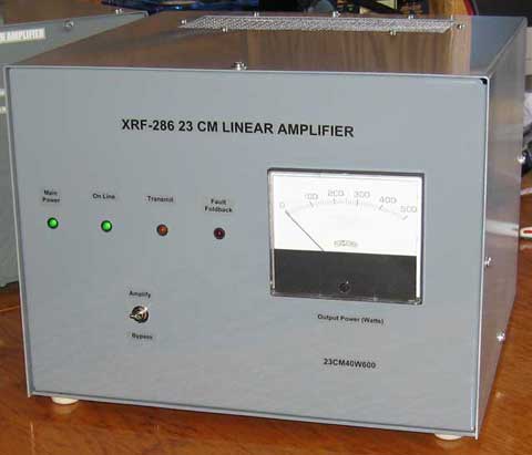
600 watts solid-state on 1296? Yes indeed.
This project began when I was lucky enough to locate some surplus XRF-286 LDMOS transistors; I thought it might be nice to have a solid-state replacement for my GS-15B amplifier, which had been in service here for 5 years.
After considerable experimenting with prototypes, the final results were terrific; with about 40w drive, it can produce 600w (saturated), and covers the entire band (1240 to 1300 MHz). It has the essential features; a quiet, temperature-controlled cooling fan, sequencer, ALC output to the driving radio, output power meter, and high VSWR fold-back protection.
I'm currently driving it with a 20w transverter to a bit over 400 out, and it just loafs along. With one of the typical 10w radios (IC-910) it still produces 200+.
Power requirements are 28v @ 48a max; at 400w out, it draws about 35a.

On the rear panel are the usual connectors; antenna and driver bulkhead N connectors, PTT in, PTT out, ALC out and a power supply connector.
There is a large screened air intake port at the rear, and another
(exhaust) in the top cover. The fan is positioned directly behind the intake
port.

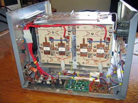
The central core of the amplifier is the heat sink cluster shown here.
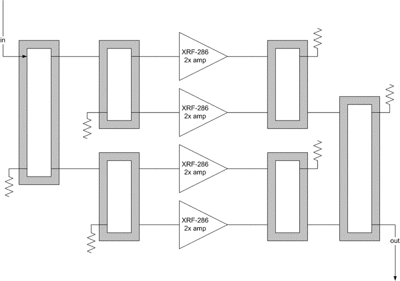
There are four amplifier boards on it, each using a pair of XRF-286's. Output from just one of these boards is in the range of 150 to 190 watts.
There is a 60cfm 120mm fan mounted at the back of the cluster, positioned to draw in cool air from the rear vent in the cabinet, and force it through the cluster fins at the center of the assembly.
Mounted to the top binding plate is a high-power 4-way
branchline hybrid coupler. There's another coupler attached to the bottom
binding plate for the input (not visible in this photo).
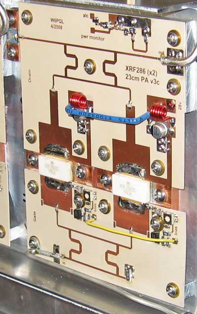
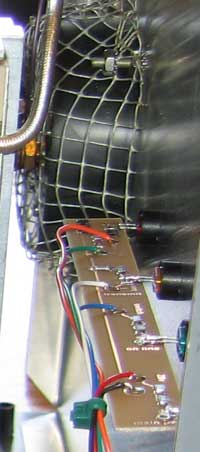
Here's a close-up of one of the prototype amplifier boards. It has it's own integrated input/output branchline hybrid couplers, and an output sampling coupler (for ALC feedback or power indication).
Each transistor has it's own bias adjustment.
The dump port on the output coupler is terminated with a 125w chip resistor (shown at upper left). If something should happen to one of the devices, the termination absorbs the imbalance, and the other device will be protected and live on.
The board material used here is Rogers Ro3006.
Note the use of 1/4" thick 2 x 2 heat spreaders under the transistors. These do a great job of drawing heat away from the devices and passing it into the heat sink below. Even at full sustained output, I can detect no drop in power level, which is a common problem when the heat spreaders are made from thinner material.
These transistors are a bit unconventional; they are made to be direct-soldered to the spreader, which had to be made from copper at a local machine shop.
The process of soldering the device to the spreader requires some courage, and should be done in an oxygen-shielded environment with special equipment (other builders report success without taking this precaution); a friend of mine in the semiconductor business handled that part for me. After that was done, I was able to treat them like a more conventional transistor, and just bolt them down to the heat sink.

Here's one mounted and ready to install. Note the slot milled into the copper
block. This sets the height of the transistor leads to the proper level for the
PC board material used, which slides under the leads onto the shelves of the
block.
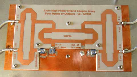 The high-power 4-way couplers
are basically three 2-port couplers
interconnected and etched onto the same microwave substrate (062 PTFE).
The high-power 4-way couplers
are basically three 2-port couplers
interconnected and etched onto the same microwave substrate (062 PTFE).
Although the insertion loss of this coupler is very low (0.2 db), at the 600 watt level the assembly has to be able to dissipate 30 watts. For this reason, a copper backplane was spot-soldered to the back side to help draw the heat into the heat sink cluster below.
This copper backplane also provides a convenient way to attach
the coax jumpers (and the 125w terminations attached to the dump ports).
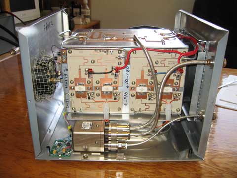
Viewing the left side now after being fully wired and tested.
There are several disconnects to the main cluster to allow for easy servicing, if necessary (just a habit of mine).
Note the space (about 1.75") at the front of the heat sink cluster; this was done to prevent restricting airflow.
Visible in the floor of the cabinet are the
sequencer and control boards, a reverse
polarity protection diode and fuse blocks.
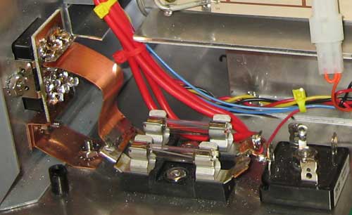 This
close-up shows the DC power input components more clearly.
This
close-up shows the DC power input components more clearly.
There is a small PC board placed over the 12-pin power connector. The board has four chip capacitors on it for RF bypassing, which is aided by the copper ground strap below it. The top-most copper strap carries the +28v to the fuse block.
The square power diode at the lower right is for those of us
who occasionally hook the + to the -. It will just blow the fuses instead of
allowing us to ruin the amp.
The small board on the front panel is used to mount the LED indicators and their supporting components.
Also shown here is the screening covering the back side of the
panel meter. No significant RF leakage there...
 The
right side of the cabinet is a bit less crowded. Visible here is the Dow-Key
transfer switch and it's relay driver board
(this is a high-power pulse-latching type of relay).
The
right side of the cabinet is a bit less crowded. Visible here is the Dow-Key
transfer switch and it's relay driver board
(this is a high-power pulse-latching type of relay).
.250 semi-rigid cable is used on the high-power side (.141 gets hot above 200w), and .141 on the input side. The inset below shows the clean transition into the output bulkhead connector using the .250 semi-rigid cable.

Note: there are pictures of other amplifiers built with the kits offered on the parts page, submitted courtesy of KD5FZX, VE4MA, and RA3AUB).
Listed below are the general block diagrams and schematics for several of the key components.
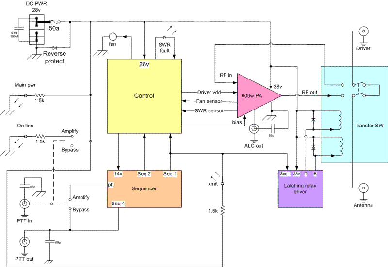

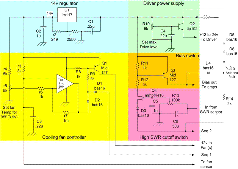
Note: the driver power supply components are not used in the amplifier described above.