
Note: the newest RF deck supplied in the kits shown here differs from the
original prototype. Here is the current schematic:
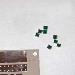 Locate
the eight 470pf MC18 mica capacitors, they will be installed on the output
board first.
Locate
the eight 470pf MC18 mica capacitors, they will be installed on the output
board first.
![]() Install
them in groups of four, mounted on their thin side as shown. Mounting them in
this way helps to even out the RF currents in each one.
Install
them in groups of four, mounted on their thin side as shown. Mounting them in
this way helps to even out the RF currents in each one.
Then mount the rest of the capacitors; the 1000pf, .01 and .1uf chip bypass caps are aligned near the transistor pads spanning the the VDD and ground traces, and the 100uf electrolytics are around the corner to the right of them. Note the polarity markings on the electrolytics.
Next, mount the two
TC12 coax transformers, beginning with the longer trimmed ends. There are 4
points to solder...the tips go to the MC18 blocking capacitor traces, and the shields
to the transistor traces.
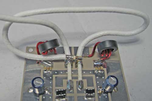 Ignore
the VDD drain chokes in these next two photos, they have been replaced with a
bifilar transformer (shown later).
Ignore
the VDD drain chokes in these next two photos, they have been replaced with a
bifilar transformer (shown later).
Loop the first coax around and rest it on top of the other exposed coax
shield connections as shown. Note the center conductor of the looped-around
coax rests on top of that coax's own shield, and the shield on top of the
opposite coax's shield. Solder into place.
 Since
we had so much fun with that first piece of coax, let's go ahead and loop the
other one around and solder it into place as well.
Since
we had so much fun with that first piece of coax, let's go ahead and loop the
other one around and solder it into place as well.
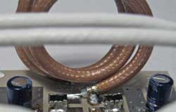
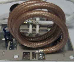 The
RG142 balun is next
The
RG142 balun is next
 Install
the bifilar VDD DC power feed transformer as shown. The short wires go to the
drain pads, and the longer ones to the bypassed vdd 50v pads.
Install
the bifilar VDD DC power feed transformer as shown. The short wires go to the
drain pads, and the longer ones to the bypassed vdd 50v pads.
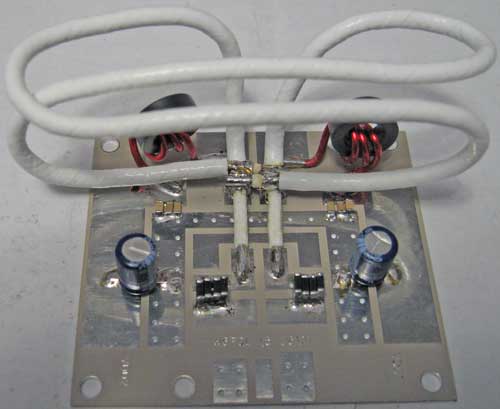
 Your
completed output board should now look like this.
Your
completed output board should now look like this.
 Now
install all the components onto the input board except for the 4 to 1 ferrite
input transformer and 4-turn gate inductor.
Now
install all the components onto the input board except for the 4 to 1 ferrite
input transformer and 4-turn gate inductor.
A high resolution photo is here:
Pre-adjust the IDQ trimmer resistor almost all the way clockwise, about a quarter of a turn. Be careful, this trimmer is fragile.
![]() Install
the input transformer, soldering it to the board at the five points
indicated.
Install
the input transformer, soldering it to the board at the five points
indicated.
 Finally,
install the 4-turn gate inductor
Finally,
install the 4-turn gate inductor
 Slide the boards under the transistor tabs (transistor should have been
previously flow-soldered to a copper spreader).
Slide the boards under the transistor tabs (transistor should have been
previously flow-soldered to a copper spreader).
Here is a video showing how to flow-solder your LDMOS to the spreader.
Here is the drilling template for the spreader.
Secure the boards to the spreader with 4-40 x 3/16 screws and flat washers. Do not over-tighten.
Use some liquid flux, and solder the boards to the LDMOS tabs as shown.
 These
final instructions refer to the degenerative feedback
components included in your kit; two 440 ohm 3w metal film resistors and
two .047uf 450v capacitors to be installed drain-to-gate (resistor/cap
in series) on each device half, as shown in the photo.
These
final instructions refer to the degenerative feedback
components included in your kit; two 440 ohm 3w metal film resistors and
two .047uf 450v capacitors to be installed drain-to-gate (resistor/cap
in series) on each device half, as shown in the photo.  Fasten
the spreader to a suitable heat sink using the guide on the right. Use a
thin but even coating of heat sink compound between spreader and heat sink.
Fasten
the spreader to a suitable heat sink using the guide on the right. Use a
thin but even coating of heat sink compound between spreader and heat sink.
Turn on the 50v main supply voltage, but not the bias; there should be no current drawn
Turn on the bias and note the idling current drawn from the 50v supply. Adjust IDQ for 2 amps. Note: the current drawn by the bias supply (usually12v) is not what you are measuring here...you must measure the idling current (IDQ) the LDMOS draws from the 50v supply.
Shut off the power supply, and remove current limiting.
Please note: if you are using a reflective low-pass filter following the output of this amplifier, be aware that third harmonic levels are high, and some danger to the LDMOS exists if this energy is not reflected back in the correct phase. For this reason, a length of RG142 (or other suitable coax type) is recommended between the output of the RF deck and the input to the filter. Some experimentation with the length may be necessary, but a general rule of thumb is to use a length that will produce at least 60% efficiency. On most installations, and using the filter I offer on the parts page, this would be about 30cm (1 ft). If the length of this stand-off coax is incorrect, you will know...the efficiency will be low (less than 60%).