Versions 6.3-6.5 are the same as version 6.2 with the exception of
adding the 20-pin header connector, and substituting wire holes in place of the
solder-to surface mount connection points.
The use of the i/o connector is optional; it was added to the board to
facilitate testing with a factory test fixture for the assembled-and-tested
product, but can also be used to make all i/o connections if you don't mind
going to the trouble to do it; this connector is
wired in parallel with the default solder-to connections in various places on the board.
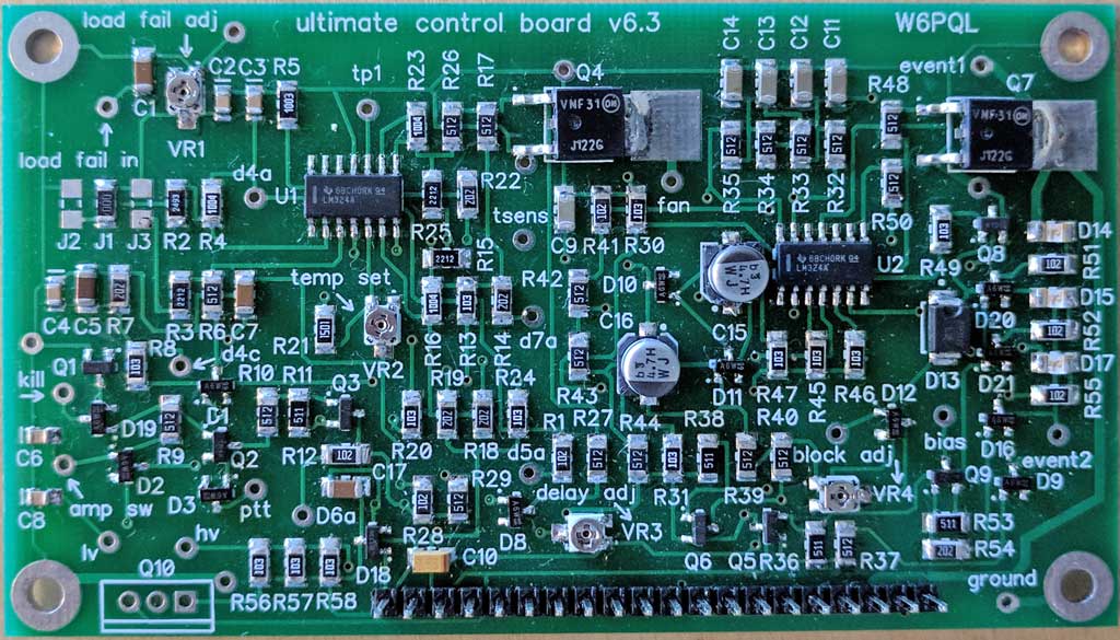
Pin 1 is on the far left, and pin 20 on the far right in the photo above.
However, investment in a crimping tool for the mating connector pins may not be
cost-effective for one-time use, so the solder-to connection holes in the PCB
may be the most practical way to connect to the board.
50-57-9020 is the manufacturer's part number for the mating connector to the
header on the PCB; 16-02-0069 is the manufacturer's part number for the pins
which go into that connector (you'll need 20).
The crimping tool used for the pins, if you don't already have one, can be
purchased for under $30 on Amazon or EBay; an alternative way is to just
spot-solder the pins to the end of your wires after crimping with long-nose
pliers.
The
header connections are as follows:
- ground
- HV; this can be up to 65v, and is the connection used to provide
12-14v from the VDD rail when Q10 will be used for that purpose. The use of
Q10 is optional, and is not used when the control board will be operated
from a 12v supply. If Q10 is to be used to provide 12v from a 28v, 50v or
65v rail, a 25 ohm 25w current-limiting resistor should be placed in series
with the connection to the rail to protect Q10 and D18 from damage due to
accidental shorting of the 12v rail (it can happen to the best of us).
Without current limiting, even a temporary short on the 12v rail will cause
that rail to permanently go to HV potential (28, 50 or 65v).
- LV; this is the 12v power input to the board; if Q10 is used, it
provides 12v to this pin, otherwise an external 12v-14v source should be
connected here.
- This is a connection to the base of Q10, and is only used for testing
with the factory test fixture.
- AMP SW; used with a front panel switch to gate 12v to the
on-board sequencer, usually to take a controlled amplifier on or off line.
- Kill port ; used to provide an immediate kill signal to an
external FET power switch to remove VDD from an amplifier during a detected
fault condition
- D6A; output to an external panel LED to indicate a transmit
condition
- PTT; input connection from a ptt control line (pull low to
energize)
- D4C; output connection to the cathode of an external LED to
indicate a fault condition caused by high reflected power (high SWR)
- D4A;output connection to the anode of the LED mentioned in #9
- Load Fail In; input connection from an external SWR sensor
- D5A; output to an external panel LED to indicate the presence of
operating power (12v rail)
- D7A; output to an external panel LED to indicate a high
temperature fault condition
- TSENS; input from an external sensor (thermistor), normally
mounted on an amplifier's heat sink
- FAN; connection to the board's fan switch, designed to pull to
ground up to 90v at up to 3 amps. Normally connected to the return lead of
cooling fan(s).
- Block; use of this signal is optional; it is a gated negative
voltage designed to be connected to a system's ALC rail going back to your
driving radio. It's purpose is to hold off any power generated by the radio,
following PTT, until the on-board sequencer has completed it's transmit
turn-on functions. This signal is released at event 3 of the on-board
sequencer.
- BIAS; sequenced amplifier bias power, 12v at up to 300ma provided
at event 2
- Event 1; a pull-to-ground connection to the first on-board
sequencer event, normally connected to antenna relay return lines. Can
switch up to 90v at up to 3 amps
- Event 2; a pull-to-ground connection to the second on-board
sequencer event, normally connected to a high current FET switch, which
gates VDD power to an amplifier's RF deck
- TP1; This is a connection to test point 1, and is used to set the
fan trigger temperature (aprox. 115F), where the fan will run continuously
until the heat sink temperature drops to about 110F. This connection should
initially be set to read 3.15K to ground when VR2 is properly adjusted and
no other connections are made to the board. This is normally set after the
board has been assembled, and before additional testing or installation.
If Q10 is to be used, it is most easily mounted by elevating the board above
the mounting surface with 3/16" spacers, passing the leads through the holes in
the board from the bottom, and securing with the appropriate mounting hardware
prior to soldering in place. The photo below shows a typical mounting. Note the
leads on Q10 do not touch the metal mounting surface below them...I made this
one uncomfortably close, the leads can be pulled up a bit more before soldering
to the board. If you will not be using Q10, you must still elevate the board
above conductive mounting surfaces a bit, as there are exposed connections on
the back of the board.

Click here for a a hi-resolution
schematic