Dual Microwave Detector Board (assembly info)
Before assembly, please read the article on sampling RF power for a full explanation about using this board.
This revision (v2) of the original dual microwave detector allows for additional customization:
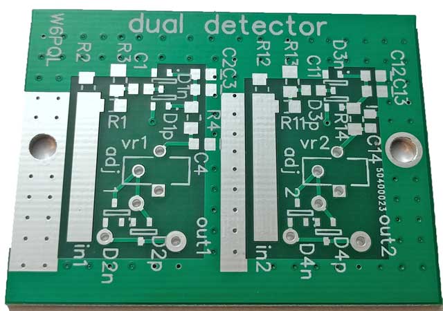
Blank PCB; note positions for negative diode configurations, and the alternate (positive) configurations. Each diode position has a default (negative, D1n-D4n) and a positive (D1p-D4p) output position.
 This
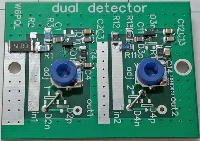
is a fully loaded board, in this case set up for the 600w 23cm amplifier used
with a 30db sampling coupler. The D2 and D4 diode positions are not normally
used in this configuration (note the jumpers bypassing the isolation diode
footprints); this is because the outputs will not be connected to anything else
that may interfere with their operation in this particular amplifier.
This
is a fully loaded board, in this case set up for the 600w 23cm amplifier used
with a 30db sampling coupler. The D2 and D4 diode positions are not normally
used in this configuration (note the jumpers bypassing the isolation diode
footprints); this is because the outputs will not be connected to anything else
that may interfere with their operation in this particular amplifier.
Nominal output voltage is 500-600mv when loaded by 5k (the value of the trimmer resistors). 5k was chosen experimentally, and provided the best linearity curves.
In some cases you may not need the 5k trimmer resistors either. For example, if you are driving the control board's load fail input port, which already has a 5k load resistor (trimmer) on it, the use of that 5k trimmer on the PCB would be unnecessary. In that case, installing a wire jumper at the trimmer resistor connections would be the correct way to configure the board.
Upon careful inspection of the diode positions, one can see this board was
set up for positive output on the left side, and negative output on the right
side...just to demonstrate how to configure for one polarity or the other.
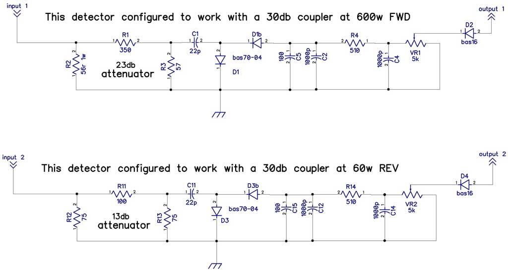
Here's the full schematic for this board; note the bypass jumpers are not shown in this diagram; the schematic also shows only the default negative output polarity.