RF Deck Information
After constructing 30+ RF decks so far, these are some of the
observations I made:
-
All of the amplifier decks were able to
produce at least 645 watts (saturated) with some of them able to
produce 700w. That's a variation of 0.3 to 0.4 db, and is normal considering
manufacturing differences from one device to another, even within the same
lot. All of the RF decks were able to achieve 600w with no more than 10w
drive. From the NXP data sheet, this is what you can expect from the best of
the lot:
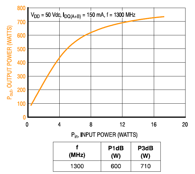
-
It should be noted this data was taken with
IDQ set to 150ma, which is OK for CW, but too low for linear operation. With
that in mind, I set IDQ to 1.5 to 1.8 amps, which produces good linearity.
-
The IDQ setting affected the input match; the
higher the IDQ, the lower in frequency the input match moved. VDD had
negligible effect on input match (from 35 to 51v).
-
Total VDD current drawn at full output varied,
with the average around 25 amps (50v VDD). Most drew a bit less than that.
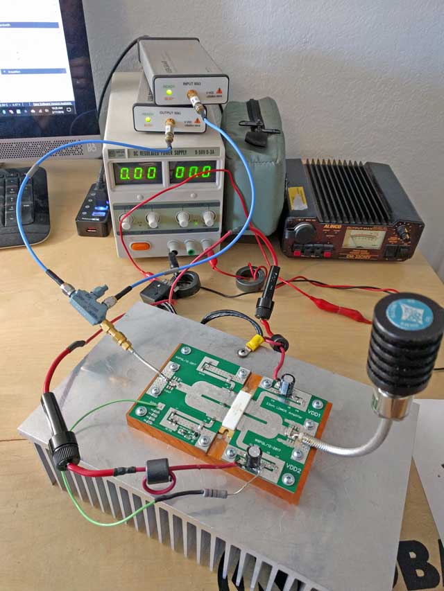
Initial testing of the deck (see test setup to
the right):
When mounting the deck, use all 8 of the supplied
4-40 machine screws and flat washers, or your metric equivalent (the washers will help distribute the
mounting forces). Get them firm, but not so tight you damage the board material,
which is soft and thin. Use heat sink compound between the copper spreader and
the heat sink...not too thick, just a thin layer will do.
All assembled/tested RF decks have already been set up in the
manner described below; no additional adjustments are necessary for operation
at 1296 MHz.
The power supply used to set up the amplifier was
current limited to 3 amps, and that's important when setting IDQ. If you are
doing this yourself with any LDMOS device on any band, and it gets away from
you, that current limiting will save the device. Fuses are not fast enough. The
termination on the output is a 30w cellular type (no drive power for this test,
of course).
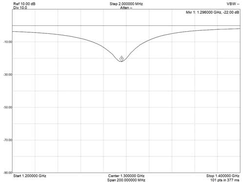
While making the IDQ setting at 50V VDD, the input
match is observed with a scalar analyzer and optimized at 1296 MHz (where most
of us will be using this). The two parameters affecting the input match were IDQ
and trimming pads. Usually, only one or two of the input trimming pads were
needed with IDQ set between 1.6 and 1.8 amps. The inset below shows the measured
optimization.
On the output side, most of the decks required
just one or two of the output trimming pads to be connected.
Making the connections to the deck
-
Both VDD traces must be connected together
when routed to your 50v rail. Wire size to each VDD trace should be at least
#16 AWG passed twice through a ferrite (Laird 28b0562-100 is recommended).
-
bias is configured for 12v (30ma current is
needed for the bias regulator on board). The resistor you see from the VDD
trace to the bias pad drops 50v down to 12v for testing. Normally, the 12v
for bias would come from a
control board
or other source, but can be derived in this way from the 50v rail as long as
the 50v is switched off when not transmitting.
-
The output coax should be able to handle the
power; SM250-50 is recommended...this is the conformable 0.25 diameter cable
you see in the photo, and is available from
www.communication-concepts.com .
-
The input coax can be most anything
with good return loss at 1296; rg316 is not very good for this, so the
recommendation is RG402 (conformable), shown in the photo above. This is available
on EBay and other places at reasonable cost. .086 or smaller conformable
coax is also OK, but usually costs more than RG402.
-
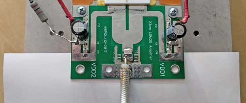 Here
are a couple of ways to connect to the input and output pads. The first is
by direct solder of the shield to the ground foil, which is difficult to do
because of the high thermal conductivity of the PC board material...the heat
is drawn away very quickly into the copper spreader, making soldering
difficult if not impossible. If you choose to do it this way, the method
shown in this photo works well. Prepare the coax so the center conductor
bends down, but does not quite touch the board when the coax outer is laid
onto the ground foil.
Here
are a couple of ways to connect to the input and output pads. The first is
by direct solder of the shield to the ground foil, which is difficult to do
because of the high thermal conductivity of the PC board material...the heat
is drawn away very quickly into the copper spreader, making soldering
difficult if not impossible. If you choose to do it this way, the method
shown in this photo works well. Prepare the coax so the center conductor
bends down, but does not quite touch the board when the coax outer is laid
onto the ground foil.
Temporarily remove the 4 screws at the end of the board, but leave the
two next to the transistor in place. Slip one or two sheets of paper
between the board and the spreader, and solder the shield to the foil, but
do not solder down the center conductor at this time. That paper will help
keep the heat from being drawn away too quickly into the copper. Remove the
paper and replace the mounting screws. Now solder the center conductor in
place. This same method can be used for the input coax connection.
 This
alternate method shows the coax pre-mounted to .020 tin mounting strips, and
because I must install coax when I set up the decks, and then remove it, it
is the method I use most of the time.
This
alternate method shows the coax pre-mounted to .020 tin mounting strips, and
because I must install coax when I set up the decks, and then remove it, it
is the method I use most of the time.
Cut your tin strips to .375 by 1.375 (3/8 by 1
3/8). Mark and drill the hole locations for pass-through (for the screws) by
comparing the strip to the board hole pattern.
Prepare your coax and solder the shield to the
tin strip, aligned as shown in the photo. Now you install your coax using
the two mounting screws at either the input or output, whichever you're
working on. Once the assembly is fastened in place, you can solder down the
center conductor.
The next page contains an
important warning about the presence of flux residue around the output
connection
The output pad has considerable microwave power on it when the amplifier
operates. It is absolutely essential to keep this area clean. The
area shown in this photo is the output pad and its trimmer pads and is the
only area on the boards requiring this special care.
 Smoke
may be the first warning as flux residue heats up, followed by small sparks
and then by a larger arc. Stopping the transmission immediately at the first
hint of trouble will prevent damage to the board, giving you time to clean
the area with isopropyl alcohol. Flux trapped under the trimming pad jumpers
has been reported to cause this kind of problem, so use just a small amount
of the no-clean type flux and clean it up afterwards.
Smoke
may be the first warning as flux residue heats up, followed by small sparks
and then by a larger arc. Stopping the transmission immediately at the first
hint of trouble will prevent damage to the board, giving you time to clean
the area with isopropyl alcohol. Flux trapped under the trimming pad jumpers
has been reported to cause this kind of problem, so use just a small amount
of the no-clean type flux and clean it up afterwards.
This also applies when you solder the output coax to this area; make certain
there is no flux in the area between the output pad and the ground plane, or
around any of the trimming pads.
Installing the PCB clamp on the RF deck
Some digital EME operators report that repetitive full power heating and
cooling (1 minute on, 1 minute off) of the rf deck in these modes will
eventually cause the thin PC board material to lift away from the heat
spreader just enough to affect the match. This is noticed when the gain and
output power drop down significantly from their usual levels, sometimes by
as much as a third. Clamping the boards securely to the heat spreader solves
this problem and restores normal function to those units affected.
Extra mounting screws could not be used for clamping due to the width and
positioning of the PCB traces, so a Teflon spacer clamping system was
developed. The sheet metal parts of the clamp system are made from
semi-rigid aluminum sheet and will self-adjust to provide the correct
pressure during heating/cooling cycles. The installation procedure is
located here:
https://www.w6pql.com/1296/pcb-clamp.htm